
ADS1x15 ADC
Overview
A 4-channel ADC module that converts analog voltage levels to digital. Uses I2C interface.
Compatible Modules
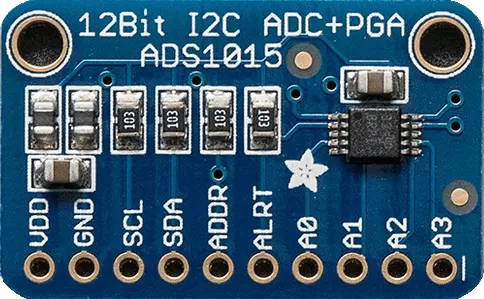
- ADS1015
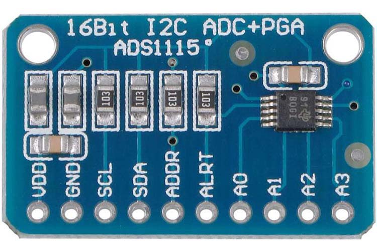
- ADS1115
Specifications (ADS1115)
- ADC Bit rate: 16 Bit.
- Interface Type: I2C.
- Channels: 4 Channel AN0 AN1 AN2 AN3 or 2 differential inputs.
- Input Voltage: 2.0 – 5.5V.
- Channel Input Voltage: 0-VDD.
- Continuous Mode: Only 150μA.
- Single-Shot Mode: Auto Shut-Down.
- Programmable Data Rate:8sps -860sps.
- Input range programmed control, 7 types input ranges: -0.256V ~ + 0.256V, -0.512V ~ + 0.512V, -1.024V ~ + 1.024V, -2.048V ~ + 2.048V, -4.096V ~ + 4.096 V, -6.144V ~ + 6.144V
• For devices with 3.3V GPIO such as Raspberry Pi, BeagleBone, Jetson Nano, etc., the VDD of ADS1x15 must be connected to 3.3V.
• ADS1x15 requires I2C signal level of approximately 70% or higher of the VDD voltage. If 5V is connected to VDD and I2C signal is 3.3V, communication errors may occur or it may not work.
• If you need to connect sensors that output 0~5V, you must use a voltage divider to convert to 0~3.3V before connecting to ADS1x15. For details, refer here.
Resolution
| Module | Single-Ended | Differential |
|---|---|---|
| ADS1015 | 0~2047 | -2047~2047 |
| ADS1115 | 0~32767 | -32767~32767 |
Supported GPIO
- Raspberry Pi 0~4
- Raspberry Pi 5
- BeagleBone Black/Green
- Jetson Nano
- FT232H, FT2232H, FT4232H
- MCP2221
Commands
[INIT]
Configures initial settings.
| Item | Type | Description |
|---|---|---|
| Module Selection | WRITE | Select the module type. (ADS1015, ADS1115) |
[SET_GAIN]
Sets the gain value.
| Item | Type | Description |
|---|---|---|
| Gain | WRITE | Select the input voltage resolution (Gain, Full scale). (2/3, 1, 2, 4, 8, 16) |
[GET_GAIN]
Reads the gain value.
| Item | Type | Description |
|---|---|---|
| Gain | READ | The currently set resolution (Gain, Full Scale). |
[READ_SINGLE]
Reads the ADC value and voltage of single ended channels.
| Item | Type | Description |
|---|---|---|
| ADC Ch0 | READ | ADC output value of channel 0. |
| ADC Ch1 | READ | ADC output value of channel 1. |
| ADC Ch2 | READ | ADC output value of channel 2. |
| ADC Ch3 | READ | ADC output value of channel 3. |
| Voltage Ch0 | READ | Input voltage calculated from channel 0 ADC output value. |
| Voltage Ch1 | READ | Input voltage calculated from channel 1 ADC output value. |
| Voltage Ch2 | READ | Input voltage calculated from channel 2 ADC output value. |
| Voltage Ch3 | READ | Input voltage calculated from channel 3 ADC output value. |
[READ_DIFF]
Reads the ADC value and voltage of differential channels.
| Item | Type | Description |
|---|---|---|
| ADC Ch0-Ch1 | READ | ADC output value of channel 0 – channel 1. |
| ADC Ch0-Ch3 | READ | ADC output value of channel 0 – channel 3. |
| ADC Ch1-Ch3 | READ | ADC output value of channel 1 – channel 3. |
| ADC Ch2-Ch3 | READ | ADC output value of channel 2 – channel 3. |
| Voltage Ch0-Ch1 | READ | Input voltage calculated from channel 0 – channel 1 ADC output value. |
| Voltage Ch0-Ch3 | READ | Input voltage calculated from channel 0 – channel 3 ADC output value. |
| Voltage Ch1-Ch3 | READ | Input voltage calculated from channel 1 – channel 3 ADC output value. |
| Voltage Ch2-Ch3 | READ | Input voltage calculated from channel 2 – channel 3 ADC output value. |
Example
Objective
Connect a potentiometer to ADS1115 and display the ADC conversion value on the dashboard widget. Turn the potentiometer knob to verify that the ADC value also changes.
Parts
| Part | Quantity |
|---|---|
| Raspberry Pi 4 * | 1 |
| ADS1115 | 1 |
| Potentiometer (Variable Resistor) | 1 |
* Other hardware can also be used. Refer to Supported GPIO.
Wiring
Connect each component to the corresponding connection as listed in each row below.
| ADS1115 | Potentiometer | GPIO |
|---|---|---|
| VDD | Pin 3 (Right) | 3.3V |
| GND | Pin 1 (Left) | GND |
| SCL | | 3 (I2C1 SCL) |
| SDA | | 2 (I2C1 SDA) |
| ADDR * | | GND |
| A0 | Pin 2 (Center) | |
* The I2C address is determined by where the ADDR pin is connected as shown in the table below. This example uses 0x48. (May vary depending on module manufacturer.)
| ADDR Pin Connection | I2C Address |
|---|---|
| GND | 0x48 |
| VDD | 0x49 |
| SDA | 0x4A |
| SCL | 0x4B |
Project Link
