MCP2221A
The MCP2221A is a USB-to-GPIO, I2C, ADC, DAC, UART converter module.
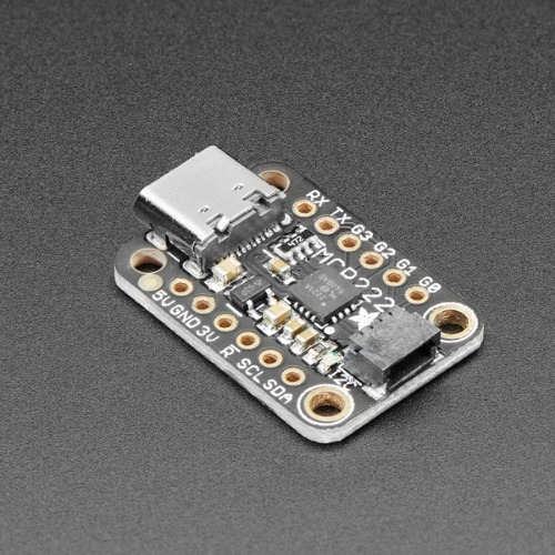
Pin Map
The name, purpose, and GPIO number of each pin are as follows:
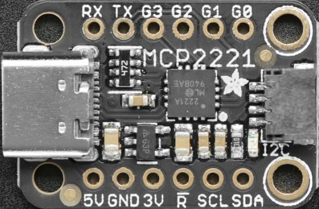
| Pin | Name | GPIO Number |
|---|---|---|
| 5V | Power | |
| 3.3V | Power | |
| GND | GND | |
| RST(R) | Reset | |
| SCL | I2C SCL | |
| SDA | I2C SDA | |
| RX | UART RX | |
| TX | UART TX | |
| G0 | GPIO0 | 0 |
| G1 | GPIO1/ADC1 | 1 |
| G2 | GPIO2/ADC2/DAC | 2 |
| G3 | GPIO3/ADC3/DAC | 3 |
Power
Pins for supplying power to connected devices (LEDs, I2C devices…) or resetting the module.
- 5V: 5V power supplied from USB.
- 3.3V: 3.3V power supplied from the internal voltage regulator.
- GND: Common GND for power and logic.
- RST: Pin for resetting the module. The module resets when LOW is applied.
I2C
Pins for I2C communication.
- SCL
- SDA
UART
Pins for UART communication. UART communication can be used through serial devices (e.g., /dev/ttyS0).
- RX
- TX
Digital I/O
4 pins can be used for digital input/output. GPIO numbers 0~3 are used.
- G0
- G1
- G2
- G3
ADC
Pins G1~G3 can be used as 10-bit (0~1023) ADC. The input voltage range is 0~3.3V or 0~5V depending on the jumper setting. (See voltage level change below)
- ADC1 (G1)
- ADC2 (G2)
- ADC3 (G3)
DAC
Pin G2 or G3 can be used as a 5-bit (0~31) DAC pin. DAC output is simultaneously output to both G2 and G3. The output voltage range is 0~3.3V or 0~5V depending on the jumper setting. (See voltage level change below)
- DAC (G2 or G3)
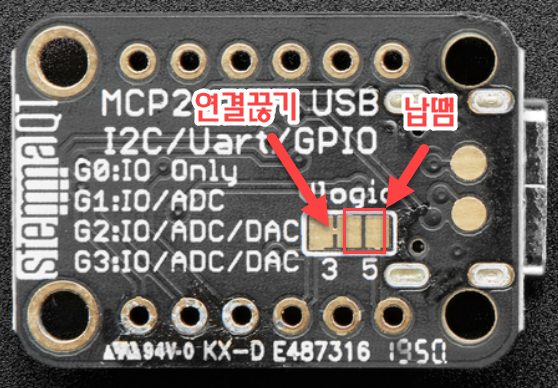
Voltage Level Change
The default voltage level for digital I/O, ADC, DAC, I2C, and UART communication is 3.3V. You can change it to 5V level by modifying the module’s jumper. As shown in the figure below, cut the 3V jumper and solder the 5V jumper on the right. (This may vary depending on the module used; described based on the Adafruit MCP2221 board)